Bezahlverfahren


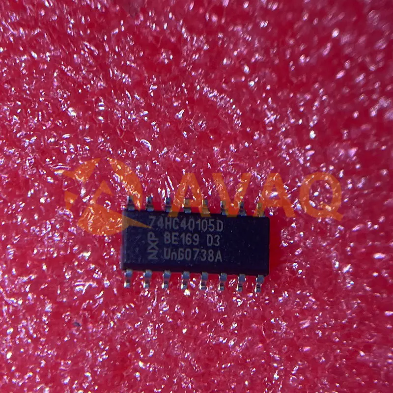
Registers 4BX16W FIFO REGISTER
SOP16Hersteller:
Herstellerteil #:
74HC40105D
Datenblatt:
Logic Type:
CMOS
Logic Family:
HC
Number Of Circuits:
Triple
Maximum Clock Frequency:
36 MHz
EDA/CAD Modelle:
All bill of materials (BOM) can be sent via email to ![]() [email protected],
or fill below form to Quote for 74HC40105D, guaranteed quotes back within
[email protected],
or fill below form to Quote for 74HC40105D, guaranteed quotes back within
![]() 12hr.
12hr.
Bitte füllen Sie das kurze Formular unten aus und wir werden Ihnen umgehend ein Angebot zukommen lassen..
INTEGRATED CIRCUITS DATA SHEET FAMILY SPECIFICATIONS HCMOS family characteristics March 1988 File under Integrated Circuits, IC06 Philips Semiconductors HCMOS family characteristics GENERAL These family specifications cover the common electrical ratings and characteristics of the entire HCMOS 74HC/HCT/HCU family, unless otherwise specified in the individual device data sheet. INTRODUCTION The 74HC/HCT/HCU high-speed Si-gate CMOS logic family combines the low power advantages of the HE4000B family with the high speed and drive capability of the low power Schottky TTL (LSTTL). The family will have the same pin-out as the 74 series and provide the same circuit functions. In these families are included several HE4000B family circuits which do not have TTL counterparts, and some special circuits. The basic family of buffered devices, designated as XX74HCXXXXX, will operate at CMOS input logic levels for high noise immunity, negligible typical quiescent supply and input current. It is operated from a power supply of 2 to 6 V. FAMILY SPECIFICATIONS A subset of the family, designated as XX74HCTXXXXX, with the same features and functions as the “HC-types”, will operate at standard TTL power supply voltage (5 V ± 10%) and logic input levels (0.8 to 2.0 V) for use as pin-to-pin compatible CMOS replacements to reduce power consumption without loss of speed. These types are also suitable for converted switching from TTL to CMOS. Another subset, the XX74HCUXXXXX, consists of single-stage unbuffered CMOS compatible devices for application in RC or crystal controlled oscillators and other types of feedback circuits which operate in the linear mode. HANDLING MOS DEVICES Inputs and outputs are protected against electrostatic effects in a wide variety of device-handling situations. However, to be totally safe, it is desirable to take handling precautions into account (see also “HANDLING PRECAUTIONS”). RECOMMENDED OPERATING CONDITIONS FOR 74HC/HCT 74HC SYMBOL PARAMETER min. typ. VCC VI VO Tamb Tamb tr, tf DC supply voltage DC input voltage range DC output voltage range 2.0 0 0 5.0 max. 6.0 VCC VCC +85 +125 1000 6.0 500 400 Note 1. For analog switches, e.g. “4016”, “4051 series”, “4351 series”, “4066” and “4067”, the specified maximum operating supply voltage is 10 V. 6.0 500 ns min. typ. max. 4.5 0 0 −40 −40 5.0 5.5 VCC VCC +85 +125 V V V °C °C see DC and AC CHAR. per device VCC = 2.0 V VCC = 4.5 V VCC = 6.0 V 74HCT UNIT CONDITIONS operating ambient temperature range −40 operating ambient temperature range −40 input rise and fall times except for Schmitt-trigger inputs March 1988 2 Philips Semiconductors HCMOS family characteristics RECOMMENDED OPERATING CONDITIONS FOR 74HCU FAMILY SPECIFICATIONS 74HCU SYMBOL VCC VI VO Tamb Tamb PARAMETER min. typ. max. DC supply voltage DC input voltage range DC output voltage range operating ambient temperature range operating ambient temperature range 2.0 0 0 −40 −40 5.0 6.0 […]
| Product Category | Registers | Logic Type | CMOS |
| Logic Family | HC | Number of Circuits | Triple |
| Maximum Clock Frequency | 36 MHz | High Level Output Current | - 7.8 mA |
| Low Level Output Current | 7.8 mA | Supply Voltage - Max | 6 V |
| Supply Voltage - Min | 2 V | Minimum Operating Temperature | - 40 C |
| Maximum Operating Temperature | + 125 C | Height | 1.45 mm |
| Input Type | Single-Ended | Length | 10 mm |
| Mounting Style | SMD/SMT | Number of Channels | 4 |
| Number of Input Lines | 4 | Number of Output Lines | 4 |
| Operating Supply Voltage | 5 V | Output Type | 3-State |
| Polarity | Non-Inverting | Product Type | Registers |
| Quiescent Current | 8 uA | Reset Type | Asynchronous |
| Factory Pack Quantity | 50 | Subcategory | Logic ICs |
| Width | 4 mm | Part # Aliases | 74HC40105D,652 |
| Unit Weight | 0.008818 oz |
After-Sales- und Abwicklungsbezogen
 Zahlung
Bezahlverfahren


Für alternative Zahlungskanäle kontaktieren Sie uns bitte unter:
[email protected] Versand & Verpackung
Versandart


AVAQ bestimmt und verpackt alle Geräte auf der Grundlage der Schutzanforderungen gegen elektrostatische Entladung (ESD) und Feuchtigkeitsempfindlichkeit (MSL)..
 Garantie

365-Tage-Produkt
Qualitätsgarantie
Wir versprechen, 365 Tage Qualitätssicherung für alle unsere Produkte zu bieten.
| Menge. | Einzelpreis | Ext. Preis |
|---|---|---|
| 1+ | - | - |
Die unten angegebenen Preise dienen nur als Referenz.


Received but not yet checked check i will add feedback