Bezahlverfahren
CDCM61002RHBR +BOM
1:2 ultra-low jitter crystal-in clock generator
VQFN-32-
Hersteller:
-
Herstellerteil #:
CDCM61002RHBR
-
Datenblatt:
-
Pbfree Code:
Yes
-
Part Life Cycle Code:
Active
-
Pin Count:
32
-
Reach Compliance Code:
compliant
-
EDA/CAD Modelle:
Verfügbarkeit: 6152 Stck
Bitte füllen Sie das kurze Formular unten aus und wir werden Ihnen umgehend ein Angebot zukommen lassen..
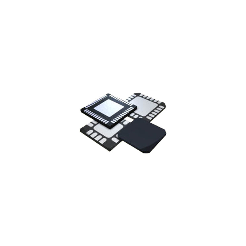
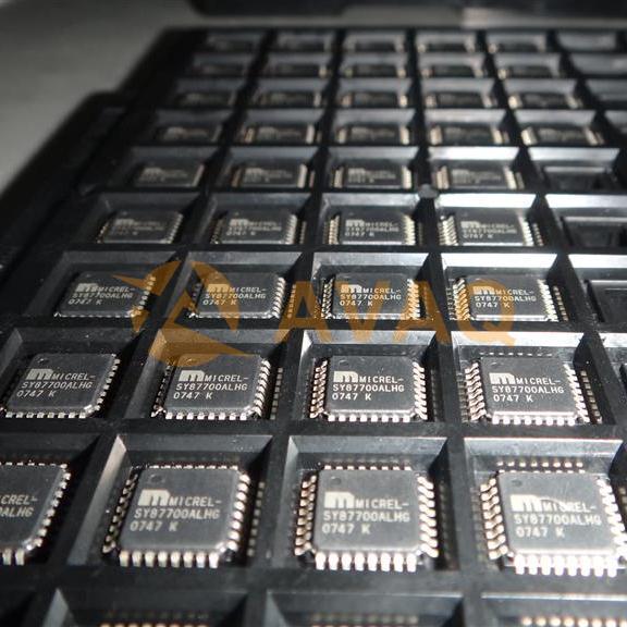
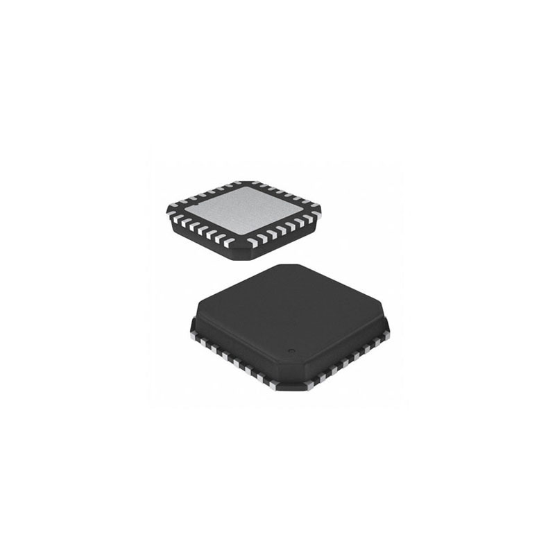
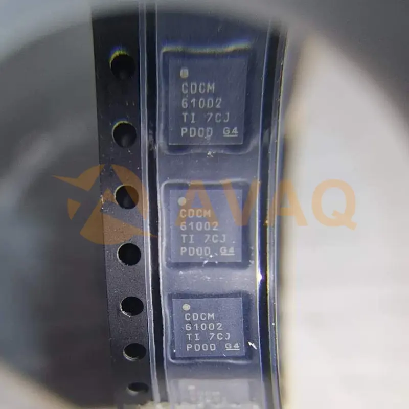
CDCM61002RHBR Allgemeine Beschreibung
The CDCM61002 is a highly versatile, low-jitter frequency synthesizer that can generate two low-jitter clock outputs, selectable between low-voltage positive emitter coupled logic (LVPECL), low-voltage differential signaling (LVDS), or low-voltage complementary metal oxide semiconductor (LVCMOS) outputs, from a low-frequency crystal or LVCMOS input for a variety of wireline and data communication applications. The CDCM61002 features an onboard PLL that can be easily configured solely through control pins. The overall output random jitter performance is less than 1ps, RMS (from 10 kHz to 20 MHz), making this device a perfect choice for use in demanding applications such as SONET, Ethernet, Fibre Channel, and SAN. The CDCM61002 is available in a small, 32-pin, 5-mm × 5-mm QFN package.
The CDCM61002 is a high-performance, low phase noise, fully-integrated voltage-controlled oscillator (VCO) clock synthesizer with two universal output buffers that can be configured to be LVPECL, LVDS, or LVCMOS compatible. Each universal output can also be converted to two LVCMOS outputs. Additionally, an LVCMOS bypass output clock is available in an output configuration which can help with crystal loading in order to achieve an exact desired input frequency. It has one fully-integrated, low-noise, LC-based VCO that operates in the 1.75 GHz to 2.05 GHz range.
The phase-locked loop (PLL) synchronizes the VCO with respect to the input, which can either be a low-frequency crystal. The outputs share an output divider sourced from the VCO core. All device settings are managed through a control pin structure, which has two pins that control the prescaler and feedback divider, three pins that control the output divider, two pins that control the output type, and one pin that controls the output enable. Any time the PLL settings (including the input frequency, prescaler divider, or feedback divider) are altered, a reset must be issued through the Reset control pin (active low for device reset). The reset initiates a PLL recalibration process to ensure PLL lock. When the device is in reset, the outputs and dividered are turned off.
The output frequency (fOUT) is proportional to the frequency of the input clock (fIN). The feedback divider, output divider, and VCO frequency set fOUT with respect to fIN. For a configuration setting for common wireline and datacom applications, refer to. For other applications, use to calculate the exact crystal oscillator frequency required for the desired output.
The output divider can be chosen from 1, 2, 3, 4, 6, or 8 through the use of control pins. Feedback divider and prescaler divider combinations can be chosen from 25 and 3, 24 and 3, 20 and 4, or 15 and 5, respectively, also through the use of control pins. shows a high-level block diagram of the CDCM61002.
The device operates in a 3.3-V supply environment and is characterized for operation from –40°C to +85°C.
Hauptmerkmale
- One Crystal/LVCMOS Reference Input Including 24.8832 MHz, 25 MHz, and
26.5625 MHz - Input Frequency Range: 21.875 MHz to
28.47 MHz - On-Chip VCO Operates in Frequency Range of 1.75 GHz to 2.05 GHz
- 2x Output Available:
- Pin-Selectable Between LVPECL, LVDS, or 2-LVCMOS; Operates at 3.3 V
- LVCMOS Bypass Output Available
- Output Frequency Selectable by /1, /2, /3, /4, /6, /8 from a Single Output Divider
- Supports Common LVPECL/LVDS Output Frequencies:
- 62.5 MHz, 74.25 MHz, 75 MHz, 77.76 MHz, 100 MHz, 106.25 MHz, 125 MHz,
150 MHz, 155.52 MHz, 156.25 MHz, 159.375 MHz, 187.5 MHz, 200 MHz, 212.5 MHz,
250 MHz, 311.04 MHz, 312.5 MHz, 622.08 MHz, 625 MHz
- 62.5 MHz, 74.25 MHz, 75 MHz, 77.76 MHz, 100 MHz, 106.25 MHz, 125 MHz,
- Supports Common LVCMOS Output Frequencies:
- 62.5 MHz, 74.25 MHz, 75 MHz, 77.76 MHz, 100 MHz, 106.25 MHz, 125 MHz,
150 MHz, 155.52 MHz, 156.25 MHz, 159.375 MHz, 187.5 MHz, 200 MHz, 212.5 MHz,
250 MHz
- 62.5 MHz, 74.25 MHz, 75 MHz, 77.76 MHz, 100 MHz, 106.25 MHz, 125 MHz,
- Output Frequency Range: 43.75 MHz to 683.264 MHz
- Internal PLL Loop Bandwidth: 400 kHz
- High-Performance PLL Core:
- Phase Noise typically at –146 dBc/Hz at 5-MHz Offset for 625-MHz LVPECL Output
- Random Jitter typically at 0.509 ps, RMS (10 kHz to 20 MHz) for 625-MHz LVPECL Output
- Output Duty Cycle Corrected to 50% (± 5%)
- Low Output Skew of 20 ps on LVPECL Outputs
- Divider Programming Using Control Pins:
- Two Pins for Prescaler/Feedback Divider
- Three Pins for Output Divider
- Two Pins for Output Select
- Chip Enable Control Pin Available
- 3.3-V Core and I/O Power Supply
- Industrial Temperature Range: –40°C to +85°C
- 5-mm × 5-mm, 32-pin, QFN (RHB) Package
- ESD Protection Exceeds 2 kV (HBM)
Spezifikationen
Source Content uid | CDCM61002RHBR | Pbfree Code | Yes |
Part Life Cycle Code | Active | Pin Count | 32 |
Reach Compliance Code | compliant | ECCN Code | EAR99 |
HTS Code | 8542.39.00.01 | Family | 61002 |
Input Conditioning | MUX | JESD-30 Code | S-PQCC-N32 |
Logic IC Type | PLL BASED CLOCK DRIVER | Moisture Sensitivity Level | 2 |
Number of Functions | 1 | Number of Inverted Outputs | |
Number of Terminals | 32 | Number of True Outputs | 2 |
Packing Method | TR | Peak Reflow Temperature (Cel) | 260 |
Surface Mount | YES | Temperature Grade | INDUSTRIAL |
Terminal Finish | NICKEL PALLADIUM GOLD SILVER | Terminal Form | NO LEAD |
Terminal Position | QUAD | Time@Peak Reflow Temperature-Max (s) | 30 |
Product Category | Clock Synthesizer / Jitter Cleaner | Series | CDCM61002 |
Number of Outputs | 4 Output | Output Level | LVCMOS, LVDS, LVPECL |
Max Output Freq | 683.28 MHz | Input Level | Crystal, LVCMOS |
Maximum Input Frequency | 28.47 MHz | Supply Voltage - Max | 3.6 V |
Supply Voltage - Min | 3 V | Minimum Operating Temperature | - 40 C |
Maximum Operating Temperature | + 85 C | Mounting Style | SMD/SMT |
Development Kit | CDCM6100XEVM | Features | Pin Programming |
Height | 0.8 mm | Length | 5 mm |
Moisture Sensitive | Yes | Operating Supply Current | 108 mA |
Operating Supply Voltage | 3.3 V | Pd - Power Dissipation | 340 mW |
Product Type | Clock Synthesizers / Jitter Cleaners | Factory Pack Quantity | 3000 |
Subcategory | Clock & Timer ICs | Width | 5 mm |
Unit Weight | 0.002547 oz |
Servicerichtlinien und andere
After-Sales- und Abwicklungsbezogen
Für alternative Zahlungskanäle kontaktieren Sie uns bitte unter:
[email protected]Versandart
AVAQ bestimmt und verpackt alle Geräte auf der Grundlage der Schutzanforderungen gegen elektrostatische Entladung (ESD) und Feuchtigkeitsempfindlichkeit (MSL)..
365-Tage-Produkt
Qualitätsgarantie
Wir versprechen, 365 Tage Qualitätssicherung für alle unsere Produkte zu bieten.
In Stock: 6.152
Minimum Order: 1
Menge. | Einzelpreis | Ext. Preis |
---|---|---|
1+ | $4,950 | $4,95 |
10+ | $4,312 | $43,12 |
30+ | $3,933 | $117,99 |
100+ | $3,548 | $354,80 |
500+ | $3,371 | $1.685,50 |
1000+ | $3,291 | $3.291,00 |
Die unten angegebenen Preise dienen nur als Referenz.
Alle Stücklisten (BOM) können per E-Mail gesendet werden an [email protected], oder füllen Sie das folgende Formular aus, um ein Angebot für CDCM61002RHBR zu erhalten. Garantierte Angebote innerhalb 12 Std.