Diese Website verwendet Cookies. Durch die Nutzung dieser Website stimmen Sie der Verwendung von Cookies zu. Weitere Informationen finden Sie in unseren Datenschutzrichtlinie.

ispGDX160VA-7B208I +BOM

High-Speed Analog and Digital Interconnects Enabled

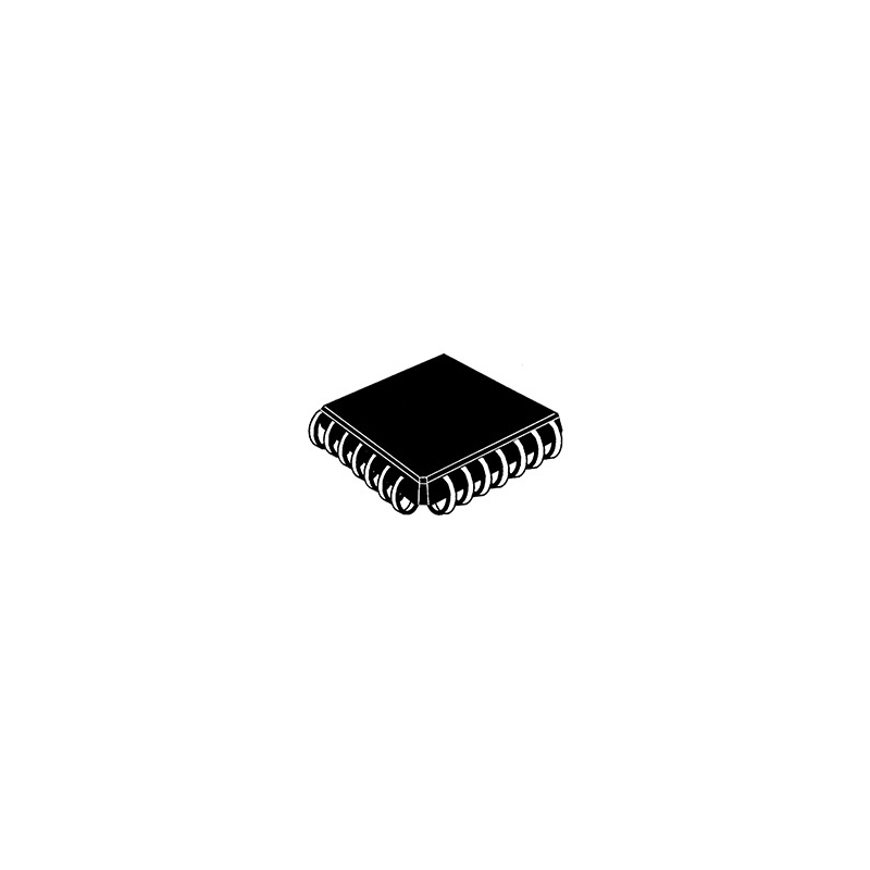
ispGDX160VA-7B208I Allgemeine Beschreibung

The ispGDXV/VA architecture provides a family of fast, flexible programmable devices to address a variety of system-level digital signal routing and interface requirements including:

• Wide Data and Address Bus Multiplexing (e.g. 16:1 High-Speed Bus MUX)

• Programmable Control Signal Routing (e.g. Interrupts, DMAREQs, etc.)

• Board-Level PCB Signal Routing for Prototyping or Programmable Bus Interfaces

The devices feature fast operation, with input-to-output signal delays (Tpd) of 3.5ns and clock-to-output delays of 3.5ns.

The architecture of the devices consists of a series of programmable I/O cells interconnected by a Global Routing Pool (GRP). All I/O pin inputs enter the GRP directly or are registered or latched so they can be routed to the required I/O outputs. I/O pin inputs are defined as four sets (A,B,C,D) which have access to the four MUX inputs found in each I/O cell. Each output has individual, programmable I/O tri-state control (OE), output latch clock (CLK), clock enable (CLKEN), and two multiplexer control (MUX0 and MUX1) inputs. Polarity for these signals is programmable for each I/O cell. The MUX0 and MUX1 inputs control a fast 4:1 MUX, allowing dynamic selection of up to four signal sources for a given output. A wider 16:1 MUX can be implemented with the MUX expander feature of each I/O and a propagation delay increase of 2.0ns. OE, CLK, CLKEN, and MUX0 and MUX1 inputs can be driven directly from selected sets of I/O pins. Optional dedicated clock input pins give minimum clockto-output delays. CLK and CLKEN share the same set of I/O pins. CLKEN disables the register clock when CLKEN = 0.

Lattice Semiconductor Corp Inventar
Lattice Semiconductor Corp Originalbestand
Lattice Semiconductor Corp Inventar

Spezifikationen

Category Integrated Circuits (ICs)LogicSignal Switches, Multiplexers, Decoders Series ispGDX®
Type Crosspoint Switch Circuit 1 x 160:160
Independent Circuits 1 Current - Output High, Low 12mA, 24mA
Voltage Supply Source Single Supply Voltage - Supply 3V ~ 3.6V
Operating Temperature -40°C ~ 85°C (TA) Mounting Type Surface Mount
Base Product Number ISPGDX160 Product Category Analog & Digital Crosspoint ICs
Product Digital Crosspoint Switches Configuration Programmable
Input Type Schmitt-Trigger, TTL Output Type 3-State, Open Drain, TTL
Operating Supply Voltage 3.3 V Minimum Operating Temperature - 40 C
Maximum Operating Temperature + 85 C Mounting Style SMD/SMT
Height 1.2 mm Length 17 mm
Moisture Sensitive Yes Product Type Analog & Digital Crosspoint ICs
Factory Pack Quantity 90 Subcategory Communication & Networking ICs
Supply Voltage - Max 3.6 V Supply Voltage - Min 3 V
Tradename ispGDX Width 17 mm
Unit Weight 0.041719 oz

Servicerichtlinien und andere

After-Sales- und Abwicklungsbezogen

payment Zahlung

Bezahlverfahren

hsbc
TT/Überweisung
paypal
Paypal
wu
Western Union
mg
Geldgramm

Für alternative Zahlungskanäle kontaktieren Sie uns bitte unter:

[email protected]
Versand Versand & Verpackung

Versandart

fedex
Fedex
ups
UPS
dhl
DHL
tnt
NTN
Verpackung

AVAQ bestimmt und verpackt alle Geräte auf der Grundlage der Schutzanforderungen gegen elektrostatische Entladung (ESD) und Feuchtigkeitsempfindlichkeit (MSL)..

Garantie Garantie

Wir versprechen, 365 Tage Qualitätssicherung für alle unsere Produkte zu bieten.

Rezensionen

You need to log in to reply. Anmelden | Melden Sie sich an