Bezahlverfahren


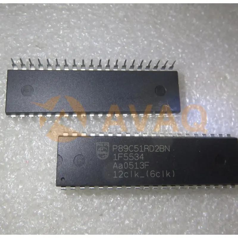
8-BIT FLASH microcontroller
DIP-40Hersteller:
Herstellerteil #:
P89C51RD2BN
Datenblatt:
Part Life Cycle Code:
Transferred
HTS Code:
8542.31.00.01
Bit Size:
8
CPU Family:
8051
EDA/CAD Modelle:
All bill of materials (BOM) can be sent via email to ![]() [email protected],
or fill below form to Quote for P89C51RD2BN, guaranteed quotes back within
[email protected],
or fill below form to Quote for P89C51RD2BN, guaranteed quotes back within
![]() 12hr.
12hr.
Bitte füllen Sie das kurze Formular unten aus und wir werden Ihnen umgehend ein Angebot zukommen lassen..
DESCRIPTIONThe 89C51RB2/RC2/RD2 device contains a non-volatile 16kB/32kB/64kB Flash program memory that is both parallel programmable and serial In-System and In-Application Programmable. In-System Programming (ISP) allows the user to download new code while the microcontroller sits in the application. In-Application Programming (IAP) means that the microcontroller fetches new program code and reprograms itself while in the system. This allows for remote programming over a modem link. A default serial loader (boot loader) program in ROM allows serial In-System programming of the Flash memory via the UART without the need for a loader in the Flash code. For In-Application Programming, the user program erases and reprograms the Flash memory by use of standard routines contained in ROM. This device executes one machine cycle in 6 clock cycles, hence providing twice the speed of a conventional 80C51. An OTP configuration bit lets the user select conventional 12 clock timing if desired.This device is a Single-Chip 8-Bit Microcontroller manufactured in advanced CMOS process and is a derivative of the 80C51 microcontroller family. The instruction set is 100% compatible with the 80C51 instruction set.The device also has four 8-bit I/O ports, three 16-bit timer/event counters, a multi-source, four-priority-level, nested interrupt structure, an enhanced UART and on-chip oscillator and timing circuits.The added features of the P89C51RB2/RC2/RD2 makes it a powerful microcontroller for applications that require pulse width modulation, high-speed I/O and up/down counting capabilities such as motor control.FEATURES• 80C51 Central Processing Unit• On-chip Flash Program Memory with In-System Programming (ISP) and In-Application Programming (IAP) capability• Boot ROM contains low level Flash programming routines for downloading via the UART• Can be programmed by the end-user application (IAP)• 6 clocks per machine cycle operation (standard)• 12 clocks per machine cycle operation (optional)• Speed up to 20 MHz with 6 clock cycles per machine cycle (40 MHz equivalent performance); up to 33 MHz with 12 clocks per machine cycle• Fully static operation• RAM expandable externally to 64 kB• 4 level priority interrupt• 8 interrupt sources• Four 8-bit I/O ports• Full-duplex enhanced UART – Framing error detection – Automatic address recognition• Power control modes – Clock can be stopped and resumed – Idle mode – Power down mode• Programmable clock out• Second DPTR register• Asynchronous port reset• Low EMI (inhibit ALE)• Programmable Counter Array (PCA) – PWM – Capture/compare
| Part Life Cycle Code | Transferred | Reach Compliance Code | |
| HTS Code | 8542.31.00.01 | Bit Size | 8 |
| CPU Family | 8051 | JESD-30 Code | R-PDIP-T40 |
| JESD-609 Code | e3 | Number of Terminals | 40 |
| Operating Temperature-Max | 70 °C | Operating Temperature-Min | |
| Qualification Status | Not Qualified | RAM (bytes) | 1024 |
| ROM (words) | 65536 | ROM Programmability | FLASH |
| Speed | 33 MHz | Supply Voltage-Nom | 5 V |
| Surface Mount | NO | Technology | CMOS |
| Temperature Grade | COMMERCIAL | Terminal Finish | Matte Tin (Sn) |
| Terminal Form | THROUGH-HOLE | Terminal Pitch | 2.54 mm |
| Terminal Position | DUAL |
After-Sales- und Abwicklungsbezogen
 Zahlung
Bezahlverfahren


Für alternative Zahlungskanäle kontaktieren Sie uns bitte unter:
[email protected] Versand & Verpackung
Versandart


AVAQ bestimmt und verpackt alle Geräte auf der Grundlage der Schutzanforderungen gegen elektrostatische Entladung (ESD) und Feuchtigkeitsempfindlichkeit (MSL)..
 Garantie

365-Tage-Produkt
Qualitätsgarantie
Wir versprechen, 365 Tage Qualitätssicherung für alle unsere Produkte zu bieten.
| Menge. | Einzelpreis | Ext. Preis |
|---|---|---|
| 1+ | - | - |
Die unten angegebenen Preise dienen nur als Referenz.
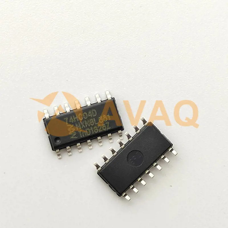
74HC04D
Toshiba
5000+ $0,072
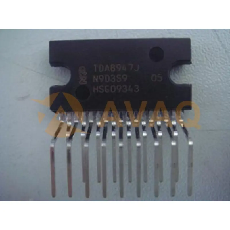
TDA8947J
NXP
Audio Amplifiers 3/4 CHANNEL AUDIO AMPLIFIER
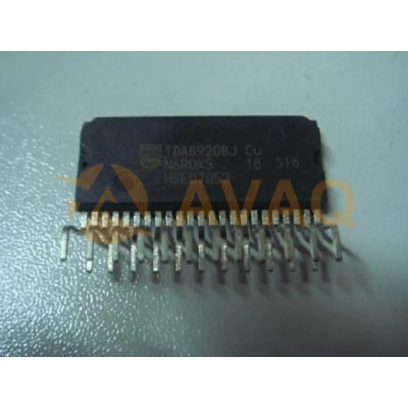
TDA8920BJ
Nxp
Experience crystal-clear sound quality and robust power handling with this efficient Class D amplifier
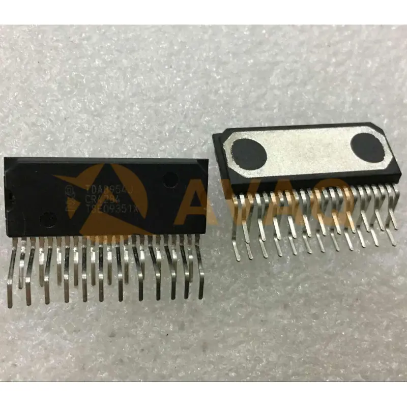
TDA8954J
Nxp
Plastic SOT411-1 PZFM23 audio amplifier
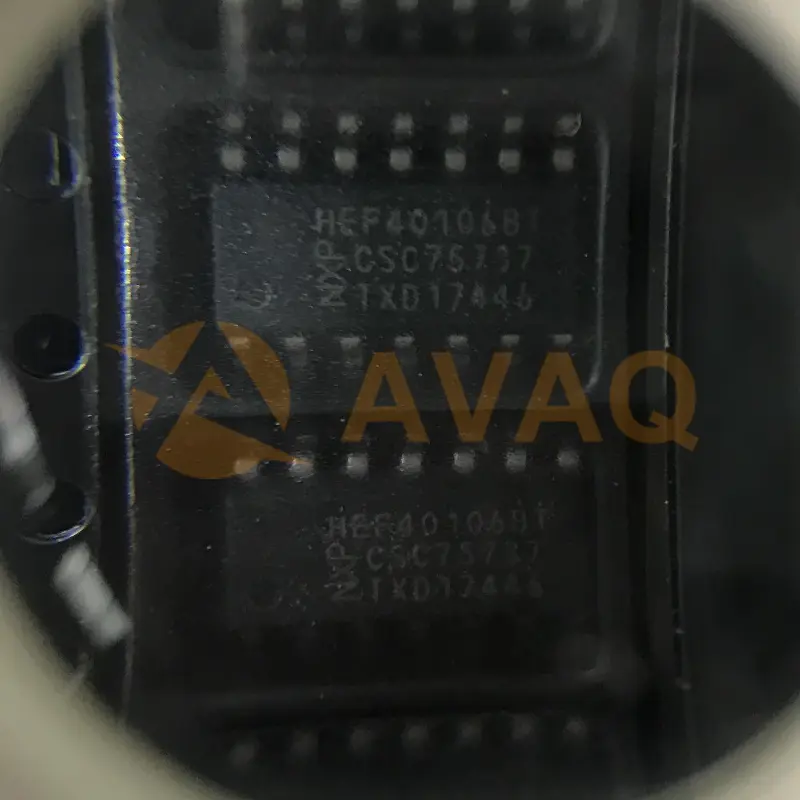
HEF40106BT
Nexperia
Inverter Schmitt Trigger 6-Element CMOS 14-Pin SO
