Bezahlverfahren


0/4 Receiver LVDS 16-SOIC
Hersteller:
Herstellerteil #:
V62/05614-01XE
Datenblatt:
Function:
Receiver
Protocols:
LVDS
Number of transmitters:
0
Number of receivers:
4
EDA/CAD Modelle:
Bitte füllen Sie das kurze Formular unten aus und wir werden Ihnen umgehend ein Angebot zukommen lassen..
This family of four LVDS data line receivers offers the widest common-mode input voltage range in the industry. These receivers provide an input voltage range specification compatible with a 5-V PECL signal as well as an overall increased ground-noise tolerance. They are in industry standard footprints with integrated termination as an option.
Precise control of the differential input voltage thresholds allows for inclusion of 50 mV of input voltage hysteresis to improve noise rejection on slowly changing input signals. The input thresholds are still no more than +50 mV over the full input common-mode voltage range.
The high-speed switching of LVDS signals usually necessitates the use of a line impedance matching resistor at the receiving-end of the cable or transmission media. The SN65LVDT series of receivers eliminates this external resistor by integrating it with the receiver. The nonterminated SN65LVDS series is also available for multidrop or other termination circuits.
The receivers can withstand ±15-kV human-body model (HBM) and ±600-V machine model (MM) electrostatic discharges to the receiver input pins with respect to ground without damage. This provides reliability in cabled and other connections where potentially damaging noise is always a threat.
The receivers also include a (patent pending) failsafe circuit that provides a high-level output within 600 ns after loss of the input signal. The most common causes of signal loss are disconnected cables, shorted lines, or powered-down transmitters. The failsafe circuit prevents noise from being received as valid data under these fault conditions. This feature may also be used for Wired-Or bus signaling. See The Active Failsafe Feature of the SN65LVDS32B application note.
The intended application and signaling technique of these devices is point-to-point baseband data transmission over controlled impedance media of approximately 100 . The transmission media may be printed-circuit board traces, backplanes, or cables. The ultimate rate and distance of data transfer is dependent upon the attenuation characteristics of the media and the noise coupling to the environment.
The SN65LVDS33-EP is characterized for operation from -55°C to 125°C.
(1) Component qualification in accordance with JEDEC and industry standards to ensure reliable operation over an extended temperature range. This includes, but is not limited to, Highly Accelerated Stress Test (HAST) or biased 85/85, temperature cycle, autoclave or unbiased HAST, electromigration, bond intermetallic life, and mold compound life. Such qualification testing should not be viewed as justifying use of this component beyond specified performance and environmental limits.
(2) The signaling rate of a line is the number of voltage transitions that are made per second expressed in the units bps (bits per second).
| Function | Receiver | Protocols | LVDS |
| Number of transmitters | 0 | Number of receivers | 4 |
| Supply voltage (V) | 3.3 | Signaling rate (MBits) | 400 |
| Input signal | CMOS, ECL, LVCMOS, LVDS, LVECL, LVPECL, PECL | Output signal | LVTTL |
| Rating | HiRel Enhanced Product | Operating temperature range (°C) | -55 to 125 |
After-Sales- und Abwicklungsbezogen
 Zahlung
Bezahlverfahren


Für alternative Zahlungskanäle kontaktieren Sie uns bitte unter:
[email protected] Versand & Verpackung
Versandart


AVAQ bestimmt und verpackt alle Geräte auf der Grundlage der Schutzanforderungen gegen elektrostatische Entladung (ESD) und Feuchtigkeitsempfindlichkeit (MSL)..
 Garantie

365-Tage-Produkt
Qualitätsgarantie
Wir versprechen, 365 Tage Qualitätssicherung für alle unsere Produkte zu bieten.
| Menge. | Einzelpreis | Ext. Preis |
|---|---|---|
| 1+ | $4,661 | $4,66 |
| 200+ | $1,804 | $360,80 |
| 500+ | $1,741 | $870,50 |
| 1000+ | $1,710 | $1.710,00 |
Die unten angegebenen Preise dienen nur als Referenz.
Alle Stücklisten (BOM) können per E-Mail gesendet werden an ![]() [email protected],
oder füllen Sie das folgende Formular aus, um ein Angebot für V62/05614-01XE zu erhalten. Garantierte Angebote innerhalb
[email protected],
oder füllen Sie das folgende Formular aus, um ein Angebot für V62/05614-01XE zu erhalten. Garantierte Angebote innerhalb
![]() 12 Std.
12 Std.
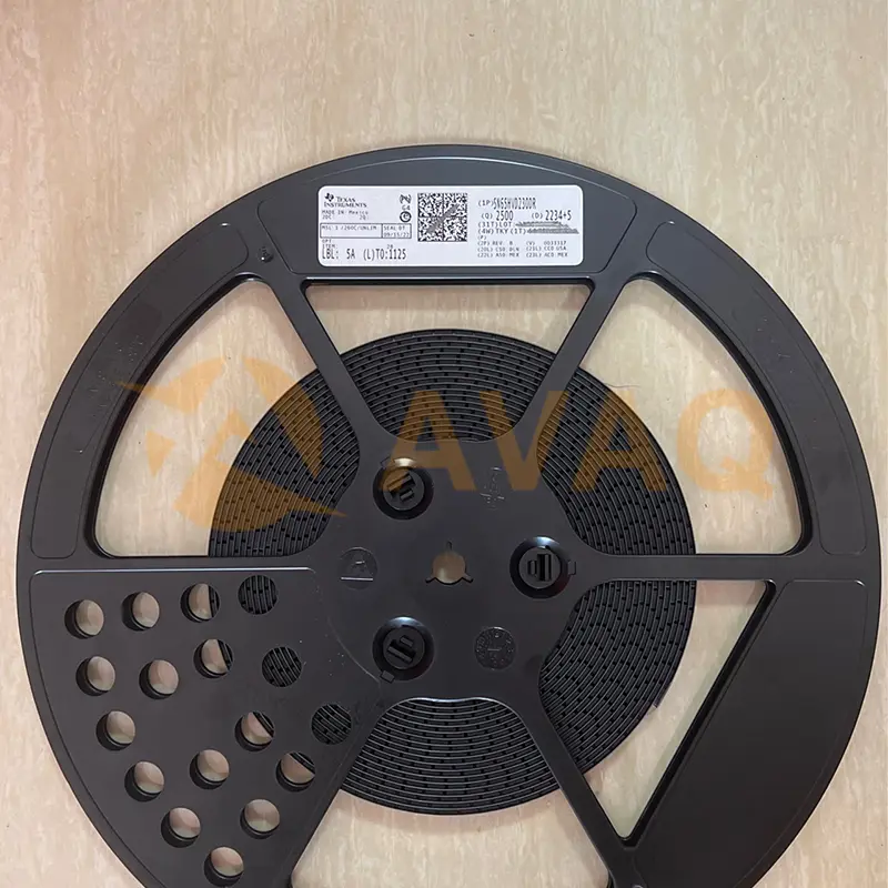
SN65HVD230DR
TI
1000+ $0,403
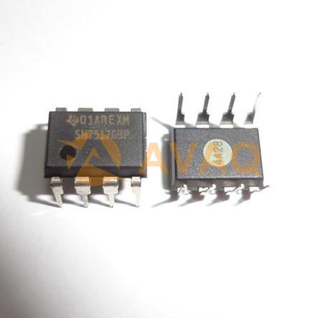
SN75176BP
Texas Instruments
1000+ $0,309

PCF8574AN
TI
8-bit 2.5- to 5.5-V I2C/SMBus I/O expander with interrupt
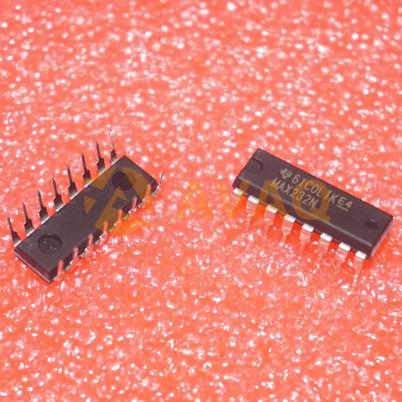
MAX232N
Texas Instruments
Dual Transmitter/Receiver RS-232 16-Pin PDIP Tube
TCA6424RGJR
Texas Instruments, Inc
24-bit translating 1.65- to 5.5-V I2C/SMBus I/O expander with interrupt, reset & config registers